Suggested PCB Land Pattern Designs For Leaded And Leadless Packages

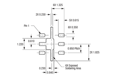
This application note provides sample PCB land pattern dimensions for a variety of leaded and leadless packages. These drawings conform with the Surface-Mount Design and Land Pattern Standard (IPC-SM-782) as published by the Institute for Interconnecting and Packaging Electronic Circuits (IPC).
Table 1 lists the land pattern drawings in this document together with their respective figure numbers. These drawings are for reference purposes only. Skyworks recommends contacting the company doing the component mounting and soldering for more information related to actual land patterns (additional dimensions, etc.).
Surface-Mount Guidelines for Leadless Packages
Skyworks plastic encapsulated leadless style packages are offered on a number of products to reduce size and weight and to improve application performance. These packages are referred to by such names as Quad Flat No-Lead (QFN), Leadless Plastic Chip Carrier (LPCC), Dual Flat No-Lead (DFN), et. al. All of them conform to JEDEC outline MO-220. As indicated in Figure 1, leadless packages use perimeter lands on the bottom of the package to provide contact with the PCB. These packages also have an exposed paddle on the bottom to provide a stable ground for optimum electrical performance of switches and attenuators, and an efficient heat path for thermal performance of amplifier products.
Get unlimited access to:
Enter your credentials below to log in. Not yet a member of RF Globalnet? Subscribe today.
