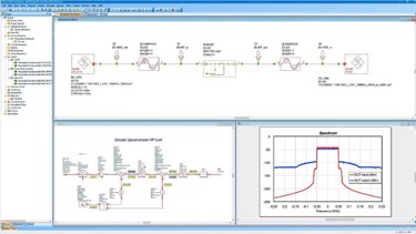
From EDA To Hardware Implementation

Your task
When designing a complex modern RF frontend or complete RF system for a 5G application or a wideband satellite link, you typically start with a simulation using an electronic design automation (EDA) tool. Obviously, you strive to minimize the number of design iterations, aiming for a first-pass design.
It is helpful to use realistic target application signals already during simulation as the latest technologies are more complex and support wider bandwidths. Ideally, you can check the resulting system level performance during simulation using key performance indicators (KPI) such as error vector magnitude (EVM) in order to enable high data throughput in the real application using the projected signals.
Previously, it was your task to connect the findings obtained with the EDA tool with later real measurements on hardware using real-world signals and standard compliant waveforms, e.g. for 5G and Wi-Fi, or user-defined wideband digital modulation schemes for satellite links.
Get unlimited access to:
Enter your credentials below to log in. Not yet a member of RF Globalnet? Subscribe today.
